


Structure determination of condensed matter samples using differential phase contrast (DPC) or center-of-mass (CoM) imaging, where variations in the CoM of the diffraction pattern map the (projected) electric field of the sample at atomic scales, has been studied extensively and well understood quantitatively [1-3] for elastic scattering within the phase-object approximation. One approach to obtaining CoM images is 4D scanning transmission electron microscopy (4D STEM), in which 2D diffraction patterns are acquired on a fast readout pixel detector at each probe position in a 2D raster scan. Placing the pixel detector behind an energy filter allows for the formation of a diffraction pattern using electrons of a particular energy loss, as depicted in Fig. 1A, and thus an inelastic counterpart of 4D STEM. Haas and Koch obtained inelastic CoM images at energy losses corresponding to inner-shell ionization and showed that they resemble elastic CoM images [4]. Here, we explore this novel imaging mode using simulation to understand the contrast observed.
We simulated energy filtered 4D STEM for inner-shell ionization energy losses using the transition matrix formulation of Brown et al. [5]. Fig. 1(B) shows the x-component CoM image for elastically scattered electrons from monolayer hexagonal boron nitride assuming 300 keV electrons and a probe-forming aperture semiangle of 15.7 mrad, and Fig. 1(C) shows the corresponding image for inelastically scattered electrons for the boron K-shell edge 10 eV above ionization threshold (188 eV). Consistent with the results of Haas and Koch [4] the elastic and inelastic images qualitatively similar. Moreover, the inelastic image does not show element-specific contrast: despite selecting the boron edge, contrast is clearly visible at the nitrogen sites. We show that in the inelastic case the DPC contrast still derives from the elastic scattering, a form of preservation of elastic contrast [6,7], modulated by the range of the ionization interaction. The appreciable contribution at nitrogen sites is a result of the delocalized interaction due to the low ionization threshold in light-element boron nitride, and is something of a special case: increasing the atomic number of the ionized atom or the energy above threshold would give more atom-specific contrast.
We further explore the dynamics of inelastic CoM imaging with sample thickness. Fig. 2(A) shows a simulated thickness-defocus tableau for elastic CoM imaging for SrTiO3 viewed along the [001] zone axis. Fig. 2(B) shows the corresponding thickness-defocus tableau for inelastic CoM imaging, assuming 10eV above the Ti L1-shell ionization threshold (564 eV). The images in the tableaus are thickness normalized, i.e. each image is divided by sample thickness, which makes clearer the structure at small thicknesses where the phase object approximation holds. Whereas elastic CoM images are only directly interpretable for thin samples (less than around 6 nm), the inelastic CoM images retain interpretable contrast reflecting the atomic structure of the specimen out to much larger thicknesses. We attribute this to the incoherent contributions from the different atoms, though show that the contribution from different atoms along the column is non-uniform, reflecting the channeling of the probe along the column [8].
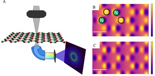
(A) Conceptual setup for collecting energy-filtered 4D-STEM data. Simulated (B) elastic and (C) inelastic CoM-x images of a monolayer of boron nitride assuming 300 keV electron and a probe-forming aperture semiangle of 15.7 mrad, and (C) further assumes an energy filter 10 eV above the boron K-edge. Despite element-specific energy filtering, both images show contrast on all columns.

Simulated (A) elastic and (B) inelastic CoM-x thickness-defocus tableaus (thickness normalized) for SrTiO3 assuming 300 keV electron and a probe forming aperture semiangle of 15.7 mrad. (B) incorporates an energy filter at 10 eV above the L1-edge. As more clearly seen in the magnified images for thickness 195 Å and defocus –100 Å, for larger thicknesses the elastic CoM-x image is no longer simply interpretable whereas the inelastic CoM-x image remains interpretable.
