


Two-dimensional (2D) materials have attracted a significant amount of attention in the last two decades, primarily due to their fascinating electronic and optical properties and their ability to be made extremely thin, down to a single atomic layer. 2D materials encompass a wide range of subgroups, including the graphene family, Xenes, transitional metal dichalcogenides (TMDC), insulators and oxides, and provide access to a vast range of materials properties. The inherent confinement of the physics to within the layers of these materials leads to remarkable changes of their properties, opening their potential use in applications such as catalysis, energy storage, nanoelectronics and optoelectronics. It is possible to deliberately tune their properties by carefully modifying the atomic structure through control of attributes such as composition, phase, thickness, and strain. For many applications, it is attractive to control these structural attributes, as the length scales decrease, within the layers to localize the interesting physics and resulting property changes. To verify and more completely understand this localization, it is important to be able to characterize the atomic structure of 2D materials with high spatial resolution and differentiate structural modifications.
Position-averaged convergent beam electron diffraction (PACBED) patterns hold a wealth of structural information about crystalline samples [1, 2]. PACBED patterns are traditionally acquired by averaging the position dependent CBED patterns while scanning an atomic resolution probe in a scanning transmission electron microscope (STEM) over at least one unit cell of the sample. The spatial averaging can be done by acquiring a single exposure diffraction pattern while quickly scanning the sample area, or by collecting a 4D STEM data set and performing post-process averaging. Extracting information from PACBED patterns is commonly done by finding the best match between an experimental pattern and a library of simulated patterns, either by visual inspection [1] or by using a quantitative metric through least squares fitting [3, 4]. These methods have several shortcomings, including comparison by eye being prone to user-bias, both methods being slow, and the fitting approach requiring the experimental and simulated patterns to be directly comparable on a pixel-by-pixel basis. Recently, it has been demonstrated that machine learning and specifically convolutional neural networks (CNNs) can use PACBED patterns to determine sample information such as sample thickness [5, 6].
In this work, we develop CNN models specifically for analyzing PACBED patterns of TMDC 2D materials with the purpose of determining various structural attributes. Simulated PACBED libraries are calculated using the frozen phonon multislice algorithm implemented in the software Prismatic 2.0 [7] for samples up to 100 nm thick in monolayer (ML) thickness steps. The CNN models are trained and implemented in Tensorflow. To create realistic training data sets like what would result from experiments, we perform random rotations, translations, small field of view changes, and other geometric transforms to the simulated patterns, and add noise according to a noise model calibrated using experimental data. These augmentations are performed on the fly during the CNN training and may easily be extended to cover other realistic variations in experimental data, eliminating the need to generate very large files with training data and enabling a larger number of training patterns.
Figure 1 shows simulated PACBED patterns from 2H MoS2, 3R MoS2 and 2H WS2 with thicknesses ranging from 10 to 165 MLs (∼100 nm). These patterns show distinct differences for a single phase at different thicknesses, for the same composition and thickness but for different phases (i.e. 2H MoS2 vs. 3R MoS2), and for the same phase and thickness but for different compositions (i.e. 2H MoS2 vs. 2H WS2). This highlights the possibility of determining thickness, phase, and composition using the features within PACBED patterns of TMDC materials. To demonstrate that CNNs can use PACBED patterns to determine structural information about 2D materials, we start with training a regression CNN model to determine the thickness of 2H MoS2. Figure 2a-b shows the relative and absolute error of this CNN model as a function of thickness. This initial result predicts that there could be <1 ML thickness error in the CNN prediction at all thicknesses between 1 ML and 165 MLs. In this study we also train classification CNNs to distinguish TMDC phase and composition, and train regression CNNs to determine the tilt between the electron probe and the sample’s c-axis. Additionally, to help design PACBED experiments and optimize CNN accuracy and precision, we explore how the prediction performance is affected by various experimental parameters, including probe convergence angle and diffraction camera length (CL) (Figure 3), as well as the effect of noise levels. Figure 3(a-c) show experimental energy-filtered PACBED patterns from 2H MoS2 at an unknown thickness acquired using three different convergence angles. Figure 3(d-g) show simulated PACBED patterns from 2H MoS2 with a 165 ML thickness acquired using four different convergence angles and five different CLs. Figure 3 illustrates that significantly different information is present in PACBED patterns acquired with different convergence angles and CLs, and therefore, these parameters could influence the CNN performance. This work demonstrates a method that can help characterize 2D material structure more completely and more accurately with a spatial resolution down to 1 unit cell. In some situations, this method could help identify structural details that are ambiguous or difficult to resolve using other methods, such as imaging, as well as possibly require a smaller total electron dose which may open measurements on beam sensitive 2D materials [8].
![Simulated PACBED patterns from (a-e) 3R MoS2, (f-j) 2H MoS2 and (k-o) 2H WS2 with thicknesses ranging from 10 MLs to 165 MLs along [0001]. These simulations used a convergence semi-angle of 26.69 mrad. The ML thicknesses are 6.13, 6.15, and 6.17 Å for 3R MoS2, 2H MoS2 and 2H WS2, respectively. For all structures, 165 MLs is approximately equivalent to 100 nm thickness. All the patterns are displayed on the same square root intensity scale. The inset patterns are cropped versions with modified intensity ranges to enhance high intensity visibility. The inset intensity ranges are the same for the patterns of the same thickness. The scale bar in (a) is 25 mrad and is true for (a-o).](https://oup.silverchair-cdn.com/oup/backfile/Content_public/Journal/mam/29/Supplement_1/10.1093_micmic_ozad067.341/1/m_ozad067.341f1.jpeg?Expires=1750390157&Signature=F1HzJ-Qos4IRarhLRhHjw9pEpj1pmOWVY-YpvvDWrjAA20wDroc9SviGOflbx2esZ1AYGr0HdTiT-T7PZTsXTywcbWQ~H4mNSNtPpcYlGgxyZ1sfg3vdOS43QicBaQQzN2bvbELZULORJ1cfWDcHef7bWzuOGZfcGaNqiurNGYP-gzO7yFQM12uCHioTATBIeQMDm0sdFKl2Fhzla40EnjhBUA10ujSzq6mbJbMKCwSeksuRiV4gSCXGqrxVKGOizQXig5CcehiI6XucIvCNiHyMyz9rDkJhO32mZKMbux61iA3ZxHoBNLLNqXqYotkZePDqWJJrHzOLh3J-7SaUJA__&Key-Pair-Id=APKAIE5G5CRDK6RD3PGA)
Simulated PACBED patterns from (a-e) 3R MoS2, (f-j) 2H MoS2 and (k-o) 2H WS2 with thicknesses ranging from 10 MLs to 165 MLs along [0001]. These simulations used a convergence semi-angle of 26.69 mrad. The ML thicknesses are 6.13, 6.15, and 6.17 Å for 3R MoS2, 2H MoS2 and 2H WS2, respectively. For all structures, 165 MLs is approximately equivalent to 100 nm thickness. All the patterns are displayed on the same square root intensity scale. The inset patterns are cropped versions with modified intensity ranges to enhance high intensity visibility. The inset intensity ranges are the same for the patterns of the same thickness. The scale bar in (a) is 25 mrad and is true for (a-o).
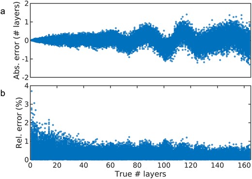
(a) Absolute and (b) relative error in thickness determination by the regression CNN model using unseen test data.
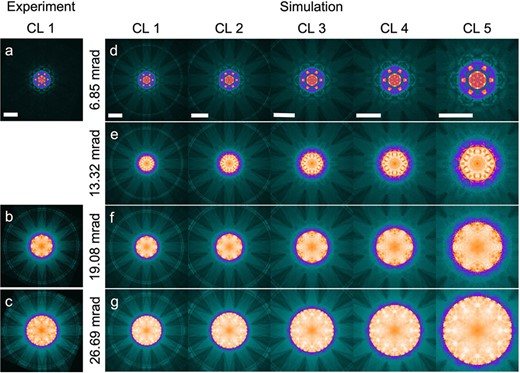
(a-c) Experimental PACBED patterns of 2H MoS2 using a convergence semi-angle of (a) 6.85, (b) 19.08 and (c) 26.69 mrad. (d-g) Simulated PACBED patterns of 2H MoS2 with a thickness of 165 MLs (∼100 nm) using a probe convergence semi-angle of (d) 6.85 mrad, (e) 13.32 mrad, (f) 19.08 mrad and (g) 26.69 mrad, and five different camera lengths (CL 1-5). Each column is a separate CL. CL 1 is similar to the one used for the experiments in (a-c). The sample thickness of the experiment and simulation are similar. Patterns are displayed on a square root intensity scale. The scale bars in the first row are all 25 mrad and are true for all the patterns of the same CL in the same column.
References
The authors acknowledge funding from the Swedish Research Council (VR, under grant No. 2020-04986), Knut and Alice Wallenberg Foundation (under grant no. 2019.0140) and from the Swedish Research Council for Sustainable Development (Formas, under grant No. 2019-01295). This work was performed in part at the Chalmers Material Analysis Laboratory (CMAL). The computations were in part performed on resources at Chalmers Centre for Computational Science and Engineering (C3SE) provided by the National Academic Infrastructure for Supercomputing in Sweden (NAISS).
