


SUMMARY
This study presents the results of an interlaboratory test designed to evaluate the accuracy of spectral induced polarization (SIP) measurements using controlled electrical test networks. The study, conducted in Germany since 2006, involved 12 research institutes, six different impedance measurement devices and four types of electrical test networks specifically designed to evaluate phase shift errors in SIP measurements. The test networks, with impedances ranging from 100 to 150 kΩ, represent high-impedance samples with different phase characteristics, and pose the measurement challenges typical of such samples, including high contact impedances and parasitic capacitances. Four key findings emerged from the study: (1) Impedance measurements across all devices showed deviations within 1 per cent over a wide frequency range (0.001–1000 Hz); (2) phase errors remained below 1 mrad up to 100 Hz for most devices, but increased at higher frequencies due to parasitic capacitances and electromagnetic coupling effects; (3) lab-specific instruments have lower phase errors than field instruments when used in a laboratory environment, primarily due to the effects of long cables and too low input impedances of the field instruments; and (4) short cables and driven shielding technology effectively minimized parasitic capacitance and improved measurement accuracy. The study highlights the usefulness of test networks in assessing the accuracy of SIP measurements and raises awareness of the various factors influencing the quality of SIP data.
1 INTRODUCTION
The spectral induced polarization (SIP) method is used to measure the complex frequency-dependent electrical conductivity of the subsurface in the mHz to kHz frequency range (Kemna et al. 2012). This method has a wide range of applications, including but not limited to ore exploration (Gurin et al. 2013; Günther & Martin 2016), estimation of saturated and unsaturated hydraulic conductivity (Binley et al. 2005; Slater 2007; Breede et al. 2011; Parr et al. 2024; Peshtani et al. 2024), bioremediation (Williams et al. 2009; Flores-Orozco et al. 2013; Saneiyan et al. 2024; Xia et al. 2025) and other biogeophysical applications (Kessouri et al. 2019; Zhang & Furman 2023; Michels et al. 2024).
A key advantage of SIP is its ability to provide detailed insights into subsurface processes, often underpinned by laboratory experiments performed under controlled conditions. These experiments involve systematically varying parameters such as water saturation, contamination levels, ore concentration and microbial activity to establish relationships between measured electrical properties and the desired parameters. However, despite its versatility, the SIP method faces challenges related to the sensitivity and accuracy of measurements, particularly in applications where the measurable effects are small compared to the achievable accuracy. These effects are typically quantified by the phase shift of the complex impedance, with the required accuracy varying across the frequency range of approximately 0.001 Hz to several hundred kHz. In some cases, an accuracy of 1 milliradian (mrad) is sufficient, whereas others demand accuracies as fine as 0.1 mrad (Zimmermann et al. 2008a). Achieving these levels of accuracy is critical, as they directly influence the reliability of scientific conclusions drawn from SIP data.
To meet the stringent accuracy requirements of SIP and fully exploit its potential, significant efforts have been devoted to improving and adapting laboratory equipment for specific applications (e.g. Zimmermann et al. 2008b; Bore et al. 2022; Gurin et al. 2022). These developments concern various components of the equipment, such as the sample holder, the coupling between electrodes and samples and the electrode geometry (Ulrich & Slater 2004; Huisman et al. 2016; Wang & Slater 2019). Among the key components of SIP systems are impedance analysers, electronic devices that measure the frequency-dependent impedance of samples. These analysers are available commercially or custom-built by research groups to meet specific laboratory needs. While commercial analysers are not necessarily designed for SIP applications, custom-built devices are often tailored to laboratory requirements and shared within the scientific community (e.g. Zimmermann et al. 2008a).
A suitable approach to test the accuracy of impedance analysers is to use electrical test networks for which the expected impedance can be theoretically calculated. These networks can be designed to mimic the specific behaviour expected for a given range of applications. Such test networks are often used during the instrument design phase (Vanhala & Soininen 1995; Zimmermann et al. 2008a), for simulating electrode impedance errors and developing as well as validating correction procedures to mitigate their effects (Huisman et al. 2016; Wang & Slater 2019) or for specific applications, such as comparing time-domain and frequency-domain measurements (Johansson et al. 2020; Martin et al. 2021) and quality control for challenging SIP applications (Ehosioke et al. 2023). Such electrical test networks are also particularly suitable for interlaboratory comparison studies in round-robin tests, as they are not as susceptible to sample contamination or destruction as other test objects (e.g. consolidated and unconsolidated porous media).
Here, we present the results of a round-robin test conducted in Germany since 2006. The test involved 12 research institutes, six impedance analysers and four types of test networks. The networks, with impedances ranging from 100 to 150 kΩ and relatively small phase shifts, were chosen to simulate high-impedance samples that pose a significant challenge for accurate SIP measurements. Originally designed to evaluate the accuracy of impedance analysers used by various working groups, the result of the round-robin test reveals broader insights into SIP measurement accuracy.
Our work comprises three main contributions:
(1) We discuss the design and accuracy of the test networks themselves, examining their suitability for various applications.
(2) We provide an overview of discrepancies between different impedance analysers and highlight the importance of accuracy in SIP applications.
(3) We identify potential sources of error, such as differences in handling practices and cable usage, and propose strategies for mitigating these issues.
In the first part of this paper, we review the fundamentals of SIP measurements, introducing the test networks and the instrumentation (and concepts) involved. Then we present the results of the round-robin test, focusing on the performances of the four test networks and discuss potential sources of error. Finally, we propose strategies to improve SIP measurement accuracy and summarize the implications of our findings for the broader scientific community.
2 MATERIALS AND METHODS
2.1 Basics of SIP measurements with impedance analysers
A general electrical model of an impedance analyser utilizing four-wire technique is shown in Fig. 1. The four-wire method is used to measure electrical impedances where cable and contact impedances can distort the measurement. Here, a known electrical current is applied to the sample through two terminals of the sample holder, while the voltage across the sample is measured using a voltmeter with a high input impedance connected to two additional terminals of the sample holder.
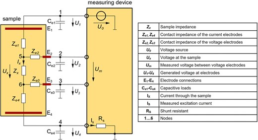
A generalized electrical network model of an SIP measurement.
Ideally, this method removes the disruptive effects of cable and electrode contact impedance, which is especially important when the contact impedance is high relative to the sample impedance. In contrast, a two-wire measurement would measure the voltage at the same contacts that are used for the current injection and would therefore also be affected by the cable and contact impedance. The contact impedance of the electrodes is frequency-dependent and can become very high at low frequencies.
The main components of the electrical model shown in Fig. 1 are the sample holder, the measuring system, and the connecting cables between them. For the sample holder, the sample impedance Zx, the contact impedances Ze1 and Ze4 of the current electrodes (including the impedances between the current and voltage electrodes), and the contact impedances Ze2 and Ze3 of the voltage electrodes are considered. The electrode connections of the sample holder are labelled E1 to E4. For the connecting cables and the measuring system, the parasitic capacitances between these cables and the ground, called capacitive loads, Ce1 to Ce4 are accounted for. Additionally, the model includes the shunt resistance Rs and the voltage source U0. The figure also shows the voltages Ux, Um and U1 to U4 as well as the currents Ix and Is that are generated when U0 is applied. Instead of a voltage source U0, a current source can also be used to inject current. In an ideal SIP measurement, the values Ux and Ix are measured to determine the exact sample impedance Zx = Ux/Ix. However, the impedance analyser can only measure the values Um (or the voltages U1 to U4) and Is, which are influenced by the abovementioned contact impedances and capacitive loads.
To mitigate the adverse effects of contact impedances, the four-wire technique is used to minimize the difference between the measured voltage Um and the desired voltage Ux. However, measurement errors (i.e. differences between Um and Ux) still occur due to the capacitive load of the cables and the measuring system. These errors typically increase with measurement frequency and become significant above a critical frequency. High contact and sample impedances in combination with the capacitive loads affect the current and the voltage measurements. For example in our test network, the capacitance Ce2 always causes the voltage U2 to be measured with an erroneous negative phase shift which distorts the actual impedance measurement. In addition to the phase-shifted voltage measurement, the Ce3 capacitance causes a leakage current which results in a phase-shifted current measurement Ix. Positive or negative phase shifts can occur depending on how the capacitances work in combination with the contact and the sample impedances. It is difficult to give a general estimate of the phase errors, as these are highly dependent on the cabling of the system, the measuring device used, and the internal calibration with any built-in correction methods. For this reason, we use test networks to assess the effect of high contact and sample impedances on the measurement accuracy and to compare the performance of SIP measuring devices.
2.2 Electrical test networks
Based on the generalized electrical model in Fig. 1, four test network types were created for evaluating measured phase errors (Fig. 2). They can be divided into two classes—class 1: TNW01, TNW02; class 2: TNW03, TNW04. For each type, two almost identical networks were available to allow parallel measurements at different institutes. The networks are built with electrical components that were measured individually with high precision. The properties of these components can be found in Table 1. The test networks were also used to develop and test suitable correction methods for current measurement and voltage measurements (Zimmermann 2011; page 18–24).

Electrical network diagrams (left) and photographs (right) of the four test networks used in the round-robin test. The size of each box is 10 cm by 5 cm.
| Test network | Set | Ze1 [Ω] | Ze2 [Ω] | Ze3 [Ω] | Ze4 [Ω] | Zx [Ω] | ||||||
|---|---|---|---|---|---|---|---|---|---|---|---|---|
| TNW01 | I | 100 000 | 0 | 0 | 100 000 | 99 400 | ||||||
| II | 100 000 | 0 | 0 | 100 000 | 98 500 | |||||||
| TNW02 | I | 100 000 | 100 000 | 100 000 | 100 000 | 100 000 | ||||||
| II | 100 000 | 100 000 | 100 000 | 100 000 | 100 000 | |||||||
| Test network | Set | Rx1 [Ω] | Rx2 [Ω] | Cx2 [nF] | Rx3 [Ω] | Cx3 [μF] | C23 [pF] | |||||
| TNW03 | I | 150 300 | 5033 | 2.2 | 9407 | 22.1 | 0.7 | |||||
| II | 139 600 | 5090 | 2.0 | 10 000 | 21.7 | 0 | ||||||
| TNW04 | I | 100 000 | 280 | 2.0 | 270 | 490 | 1.8 | |||||
| II | 98 700 | 281 | 2.0 | 270 | 470 | 0 | ||||||
The first class consist of the two network types named TNW01 and TNW02 that are used to test the effect of electrode contact impedances on SIP measurement accuracy. Network type TNW01 represents a pure resistive sample with a high impedance and high contact impedances Ze1 and Ze4 for the current electrodes. Network TNW02 represents the same resistive sample, but this time the contact impedances at the current electrodes, Ze1 and Ze4, and the potential electrodes, Ze2 and Ze3, are high. Ideally, only the sample impedance Zx of about 100 kΩ should be measured for both networks with zero phase response.
The TNW01 network can be used to test current measurement errors due to capacitive leakage currents, regardless of the excitation used. In some systems, this error can be corrected by internal calibration or correction methods if the load capacitances, Ce3 and Ce4, are known. In addition to the phase error, the noise or 50 Hz interference can be tested, which can be coupled in capacitively, especially for high resistances. Since the electronic components have finite accuracy, the impedance values Zx for TNW01 were determined independently with higher accuracy, which is why they deviate from their nominal value of 100 kΩ.
The TNW02 network causes a voltage measurement error in addition to the current measurement error, which leads to significantly greater measurement problems, as discussed and shown in Huisman et al. (2016). In contrast to the correction of the current measurement that only requires knowledge of the load capacitances, the correction of the voltage measurement also requires knowledge of the contact impedances. To improve measurement accuracy, it is important to reduce the load capacitance of the cables and the system as much as possible because these capacitances lead to distortions often referred to as parasitic effects. One strategy to minimize this capacitance is to use triaxial cables with driven shield technology (e.g. Zimmermann et al. 2008a), which is feasible for laboratory SIP equipment with short cables (up to 1 m).
The second class of electrical networks is designed to reflect the typical phase response of a soil or rock sample. This network only contains the sample impedance Zx, which is made up of individual electrical components without further contact impedances. With network TNW03, which is identical to the one used in Vanhala & Soininen (1995), a spectrum with two phase peaks at about 1 Hz and 14 kHz is obtained. The phase response of the low frequency peak is relatively strong with a phase of ∼30 mrad. However, the high frequency phase peak is overlaid by the effect of the parasitic capacitances (a decay of the amplitude and an increase of the phase shifts at high frequencies), which is essentially a low pass filter behaviour. To demonstrate this filtering effect, the parasitic capacitance of C23 = 0.7 pF between electrode 2 and 3 in TNW03 is modelled in set I only (Figs 5b, e, h—theory curve I). The comparison of the two sets (theory curves I and II in Fig. 5) shows that the phase response due to the parasitic capacitance will dominate at frequencies above 1 kHz.
A second network type in this class was also realized, TNW04. It has two phase peaks at about 1 and 300 Hz. The two phase peaks are small with peak values between 1 and 2 mrad. As with TNW03, the model is calculated once with and once without the parasitic capacitance. With these two networks, phase measurements in the entire spectrum are tested. Given that the contact impedances at the potential electrodes are not considered, they pose a less stringent test for the SIP measurement equipment.
2.3 Instruments and measuring concepts
Typically, impedance analysers use the four-wire technique and determine the impedance values with voltage and current measurements (Fig. 1). The voltages are measured at the sample with high-impedance amplifiers and analogue-to-digital converters (ADC). The current values are measured at a shunt resistor. The current flows through the shunt resistor and the resulting voltage at the shunt resistor is recorded with high-impedance amplifiers and ADC. Voltage or current sources are used for excitation. This measurement approach is well suited for complex impedance measurements from DC (µHz or mHz) up to several 100 kHz.
In the following, we briefly introduce the systems that were used within the round-robin test.
2.3.1 Device A
The SIP measurement Device A (Zimmermann et al. 2008a) consists of a function generator, an amplifier unit, a data acquisition card and a computer. The function generator produces a sine wave stimulation voltage with adjustable amplitude and frequency. The voltages at the potential electrodes of the sample are measured with short triaxial cables (using driven shield technique) and a high impedance DC coupled amplifier to minimize the capacitive loads Ce1 to Ce4 and leakage currents (Fig. 1). The input resistance and capacitance are approximately 500 GΩ and 5 pF. The current is determined by measuring the voltage across an adjustable shunt resistor (typically 1 kΩ) connected in series with the sample impedance. The voltages at the shunt resistor and those at the potential electrodes of the sample are digitized using high resolution ADC. By applying the lock-in technique, the complex amplitudes of the voltages for the measurement frequency are determined from the measured time-series. The lock-in technique uses the Fourier transformation to calculate the signal for the measurement frequency only and suppresses all other signal components. Finally, the impedance of the sample is determined from these complex amplitudes, with additional corrections for measurement errors due to signal propagation times and parasitic leakage currents. With this system, measurements can be made in the frequency range between 1 mHz and 45 kHz using an excitation voltage up to 10 V. To achieve the highest possible measurement accuracy, the system should be calibrated by taking measurements on a calibration network. It should be noted that the use of incorrect calibration values can lead to significant errors. To evaluate the adequacy of the calibration, measurements should be carried out on test networks. To correct the current measurement, the capacitance values of the capacitive loads Ce1 to Ce4 are pre-defined but can be adjusted during post-processing if additional capacitances from the sample holder are identified.
2.3.2 Devices B, C and D
The underlying measurement concept of the devices B, C and D is similar to that shown in Fig. 1 (Radic-Research, Germany). The SIP response is measured by applying sinusoidal wave currents at different frequencies. The excitation current is calculated from the voltage measured across a shunt resistor. The voltages are also recorded as a time-series synchronously with the current measurement. Finally, the complex frequency-dependent electrical impedance is calculated from the measured time-series according to magnitude and phase for the individual frequency values of the spectrum. The complex impedances and the associated confidence intervals are calculated using a discrete Fourier transform (Radic 2007).
Device B is the SIP-FUCHS-III field instrument. In this system, the transmitter, current receiver and voltage receiver are housed in separate enclosures. Fibre-optic cables are used for synchronization and signal transmission to the receivers (cable lengths up to 200 m). In this way, this device offers flexibility in the design of the measurement arrangement, which is very advantageous for field applications. The frequency range of the SIP-FUCHS-III is 1 mHz to 20 kHz. The instrument is equipped with active shielding of the potential cables. In this way, the influence of the cable capacitance on the voltage measurement can be almost completely suppressed. The actively shielded potential cables and the flexible design of the current cable lengths make this field measuring device suitable for laboratory use.
Device C is the SIP256C field instrument. It is optimized for field measurements with a dipole–dipole configuration. The measurement channels are housed in individual Remote Units (RU). Each RU can be used for both current and voltage measurements. In the field, the RUs are connected to form a chain and spaced at intervals of 0.5–10 m. The frequency range of the SIP256C is 1 mHz to 1 kHz. As the RUs have no active shielding, they can only be used for laboratory measurements in the low-frequency range. The Remote Reference Units (RRUs) available for the SIP256C are more suitable for laboratory applications. They are similar in design to the units of the SIP-FUCHS-III and also have active shielding of the potential cables. The RRUs are used in the field to detect and suppress interference voltages that can reduce data quality (Radic 2014). However, the SIP256C's operating software also allows it to be used for laboratory measurements. One RRU is then used for voltage measurement and the other for current measurement. Only these RRUs were used for the measurements on the test networks. Compared to Device B, the available frequency range is limited to 1 kHz. In addition, the capacitance of the pre-amplifiers is about one order of magnitude higher than for Devices B and D, which affects the measurement accuracy at the high frequency end.
Device D is the SIP-QUAD which has been specialized designed for laboratory applications. It features an extended frequency range spanning from 10 µHz to 230 kHz. A key advantage of the SIP-QUAD is its use of active pre-amplifiers (probes) placed directly at the current and potential electrodes of the sample holder. This design minimizes the input impedance to 1 pF, significantly enhancing measurement accuracy, particularly at high contact resistances and high frequencies. The device enables simultaneous measurements of up to four material samples, each equipped with a dedicated signal source (±10 V, ±10 mA) and separate current and voltage measurement channels. If required, the four separated voltage channel pairs can be linked to a single signal source, facilitating tomographic measurements with one current dipole and seven voltage dipoles. This device allows also frequency combinations in a multifrequency excitation mode, enabling the entire impedance spectrum to be captured in a single measurement process with maximum efficiency.
2.3.3 Device E
Device E is the PSIP, a multichannel geophysical instrument optimized for laboratory and in-situ near surface SIP (Ontash & Ermac, USA). It measures conventional resistivity, time- and frequency-domain induced polarization as well as self-potential following the measurement principles outlined in Fig. 1. The SIP response is measured by applying sine wave voltages at different frequencies. The impedance and phase are determined by correlating induced voltage and stimulus current. The stimulus current is computed based on the voltage measured at a shunt resistor using Ohm's law. The main application areas of Device E are laboratory investigations and small-scale surface and shallow borehole field environments. It measures in the frequency range between 1 mHz and 20 kHz with up to 4 simultaneous setups. It has an actively driven electrode guards/shields to mitigate capacitive coupling and noise. The voltage output is ±10 V and the current is 10 mA per channel. The input impedance of the voltage channels is greater than or equal to 1 GΩ.
2.3.4 Device F
Device F is the VMP3-Z (Princeton Applied Research, USA; distributed by BioLogic, USA), which was designed for electrochemical applications of impedance spectroscopy, and has also been used for petrophysical measurements for 15 yr. The instrument can be operated in galvanostat and potentiostat mode, that is, that either holds the current constant and measuring the potential, or vice versa. A specific electrical circuit diagram is not available, but it can be assumed that the principle follows the standards of potentiostat/galvanostat measurements. A low-current option is available specifically for high impedance applications. Measurements can be done in the frequency range between 0.01 Hz and 1 MHz. The input impedance for the normal and low-current measurement option are specified as 1012 and 1014 Ω, respectively. The stray capacitance is specified as 20 pF (normal) and 3 pF (low-current). The measurements reported here were made with the standard four-wire configuration, in galvanostat mode with the low-current option.
An overview of the different instruments and the colour-coding used in the results presented can be found in Table 2.
Overview of the instruments used, including links to the manufacturers.
| Study name | Instrument name | Manufacturer | Figure colours |
|---|---|---|---|
| Dev A | SIP-ZEL | FZ Jülich1 |  |
| Dev B | SIP-FUCHS-III | Radic Research2 |  |
| Dev C | SIP256C | Radic Research |  |
| Dev D | SIP Quad | Radic Research |  |
| Dev E | PSIP | Ontash & Ermac3 |  |
| Dev F | VMP | Princeton Applied Research4 |  |
Overview of the instruments used, including links to the manufacturers.
| Study name | Instrument name | Manufacturer | Figure colours |
|---|---|---|---|
| Dev A | SIP-ZEL | FZ Jülich1 | |
| Dev B | SIP-FUCHS-III | Radic Research2 | |
| Dev C | SIP256C | Radic Research | |
| Dev D | SIP Quad | Radic Research | |
| Dev E | PSIP | Ontash & Ermac3 | |
| Dev F | VMP | Princeton Applied Research4 | |
2.4 Participating institutes
The German Geophysical Society (DGG) hosts an Induced Polarization (IP) working group called AKIP 1. Almost all German universities, research institutes and companies interested in IP are members of this group. The AKIP meets twice a year, organizes national IP workshops every two years (alternating with the international IP workshop), maintains an SIP archive2, and exchanges news, data and the latest developments in the German IP community. For more than 15 yr, interlaboratory comparisons have been carried out with the above-described test networks, sandstone specimens and sample holders. During this time, almost all German institutes have joined. In addition, St. Petersburg State University in Russia and Lund University in Sweden have also participated. The institutes listed in Table 3 have provided data for this study.
Overview of the participating institutes. Institutes with symbols in different colours have measured the test networks with several devices (colour code in Table 2).
| Study name | Institute | Contact person | Figure symbols |
|---|---|---|---|
| Inst 1 | BAM—Bundesanstalt für Materialforschung und -prüfung | Sabine Kruschwitz |  |
| Inst 2 | BGR—German Federal Institute for Geosciences and Resources | Stephan Costabel |  |
| Inst 3 | TUC—Technical University Clausthal | Andreas Weller |  |
| Inst 4 | FZJ—Forschungszentrum Jülich | Egon Zimmermann |  |
| Inst 5 | RWTH—Aachen University | Norbert Klitzsch |  |
| Inst 6 | LIAG—Institute for Applied Geophysics | Matthias Halisch |  |
| Inst 7 | SPBU—St. Petersburg State University | Konstantin Titov |  |
| Inst 8 | TUB—Technische Universität Berlin | Sabine Kruschwitz |  |
| Inst 9 | TUBAF—Technical University Bergakademie Freiberg | Jana Börner |  |
| Inst 10 | LU—Lund University | Tina Martin |  |
| Inst 11 | EKUT—Eberhard Karl University Tübingen1 | Adrian Mellage |  |
| Inst 12 | TUBS—Technical University Braunschweig | Andreas Hördt |  |
| Study name | Institute | Contact person | Figure symbols |
|---|---|---|---|
| Inst 1 | BAM—Bundesanstalt für Materialforschung und -prüfung | Sabine Kruschwitz | |
| Inst 2 | BGR—German Federal Institute for Geosciences and Resources | Stephan Costabel | |
| Inst 3 | TUC—Technical University Clausthal | Andreas Weller | |
| Inst 4 | FZJ—Forschungszentrum Jülich | Egon Zimmermann | |
| Inst 5 | RWTH—Aachen University | Norbert Klitzsch | |
| Inst 6 | LIAG—Institute for Applied Geophysics | Matthias Halisch | |
| Inst 7 | SPBU—St. Petersburg State University | Konstantin Titov | |
| Inst 8 | TUB—Technische Universität Berlin | Sabine Kruschwitz | |
| Inst 9 | TUBAF—Technical University Bergakademie Freiberg | Jana Börner | |
| Inst 10 | LU—Lund University | Tina Martin | |
| Inst 11 | EKUT—Eberhard Karl University Tübingen1 | Adrian Mellage | |
| Inst 12 | TUBS—Technical University Braunschweig | Andreas Hördt | |
The instrument is now at the University of Kassel, Germany but the contact person remains the same.
Overview of the participating institutes. Institutes with symbols in different colours have measured the test networks with several devices (colour code in Table 2).
| Study name | Institute | Contact person | Figure symbols |
|---|---|---|---|
| Inst 1 | BAM—Bundesanstalt für Materialforschung und -prüfung | Sabine Kruschwitz | |
| Inst 2 | BGR—German Federal Institute for Geosciences and Resources | Stephan Costabel | |
| Inst 3 | TUC—Technical University Clausthal | Andreas Weller | |
| Inst 4 | FZJ—Forschungszentrum Jülich | Egon Zimmermann | |
| Inst 5 | RWTH—Aachen University | Norbert Klitzsch | |
| Inst 6 | LIAG—Institute for Applied Geophysics | Matthias Halisch | |
| Inst 7 | SPBU—St. Petersburg State University | Konstantin Titov | |
| Inst 8 | TUB—Technische Universität Berlin | Sabine Kruschwitz | |
| Inst 9 | TUBAF—Technical University Bergakademie Freiberg | Jana Börner | |
| Inst 10 | LU—Lund University | Tina Martin | |
| Inst 11 | EKUT—Eberhard Karl University Tübingen1 | Adrian Mellage | |
| Inst 12 | TUBS—Technical University Braunschweig | Andreas Hördt | |
The instrument is now at the University of Kassel, Germany but the contact person remains the same.
3 RESULTS
All participating institutes measured the first three electrical test networks (TNW01-TNW03). Network TNW04 was measured by only a few of the institutes as it was designed at a later stage. The test networks were measured at different institutes and by different users. Some of the users are more experienced and trained than others, and we expect that the differences in the results also include variability due to user training. In addition, the laboratory environments at the different institutes vary in terms of noise, shielding or additional equipment around the impedance analyser (e.g. cables, tables and climate chamber). We assume that the test results presented here also reflect the variation to be expected from different laboratory conditions. Figs 3–6 show the measurement results for each test network. In all four figures, the top row shows the data for Device A, the middle row shows the data for Devices B, C and D and the bottom row for Devices E and F. In each row, the resistance (a, d, g) and phase shift (b, e, h) are shown for the entire (instrument-specific) frequency range and additionally a close-up of the phase shift in the frequency range from 0.001 to 100 Hz is shown (c, f, i).
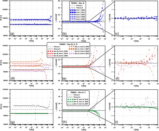
SIP results for test network TNW01 for several devices (dev) and institutes (Inst) in different years. Left column (a, d, g): resistance. Middle column (b, e, h): phase values for the entire (instrument-specific) frequency range. Right column (c, f, i): phase values for a selected frequency range. Top row: Device A. Middle row: Devices B, C, D; Bottom row: Devices E and F.
The results for TNW01 are shown in Fig. 3. The two versions of this test network are expected to have an impedance of 99.4 and 98.5 kΩ, respectively, and a phase shift of 0 mrad (Table 1). The parasitic capacitances introduce a current measurement error that must be compensated for by internal correction methods in each system. For this reason, the phase values of devices with internal current correction are seen to fluctuate around zero at high frequencies. All instruments and institutes measured the impedance value within 1 per cent deviation (Figs 3a, d, g) although some instruments start to deviate more at frequencies above 1000 Hz (Device B, C, D and F). The phase shift values were <1 mrad for most of the instruments in a frequency range of roughly 0.001–100 Hz (Figs 3b, e, h). When measuring with Devices A and E, the fluctuation in the phase spectrum (‘noise’) is in the range of 0.1 mrad for frequencies up to 100 Hz (Figs 3c, f, i). Device F shows a significant higher noise level in the same frequency range (noise peaks up to 1 mrad, Fig. 3i). For Devices B, C and D, the noise level is difficult to estimate since the noise is overlayed with the frequency-depended phase shift (Fig. 3f). In addition, the measurement with Device F shows a 50 Hz peak (Fig. 3g), most likely due to the 50 Hz power supply system. Experience suggests that the other measurement systems would also have shown a distortion at 50 Hz if measurements had been taken at exactly this frequency. Compared to the measurements with Devices B, C and F, the measurements with Devices A, D, E show significantly lower phase errors in the upper frequency range, and errors are only visible above 1000 Hz.
The results for test network TNW02 (Fig. 4) show a similar behaviour to test network TNW01. Again, the expected theoretical response is a constant impedance of 100 kΩ and zero phase shift. The impedance is measured to within 1 per cent deviation and the measured phase shifts are mostly <1 mrad in the frequency range between 0.001 and 100 Hz for Devices A, D, E and F. For Devices B and C, the phase error starts to increase already at lower frequencies. As expected, the phase errors are predominantly negative. This is due to the contact impedances at the voltage electrodes, represented by Ze2 and Ze3 in combination with the parasitic capacitances. To correct this error, it is necessary to determine the contact impedances in addition to the parasitic capacitances, which is much more complicated. These measurements clearly show that parasitic elements can lead to large phase errors. Due to the additional contact impedances of TNW02, the phase errors in the current measurement can be offset by the phase errors in the voltage measurement, as observed by device E from institute 11 (Fig. 4h). As a result, the individual errors are no longer distinguishable.

SIP results for test network TNW02 for several devices (dev) and institutions (Inst) in different years. Left column (a, d, g): resistance. Middle column (b, e, h): phase values in the entire (instrument-specific) frequency range. Right column (c, f, i): phase values for a selected frequency range. Top row: Device A; Middle row: Devices B, C, D; Bottom row: Devices E and F.
Test network TNW03 is characterized by two phase peaks at about 1 Hz and 14 kHz (Fig. 5). The low frequency peak is relatively strong with an expected phase of 32 mrad but the high frequency phase peak is overlaid by the low pass behaviour of the network and is therefore hardly recognizable. The measurements from all instruments and institutions showed that the impedances of the test network TNW03 were measured with an accuracy of 1 per cent as in the previous measurements (Figs 5a, d, g). In addition, the low frequency peak of the measured phase was located at the appropriate frequency and with the correct phase magnitude (Figs 5c, f, i). However, the phase errors occurred at lower frequencies, starting partly already at 10 Hz (Figs 5f and i).

SIP results for test network TNW03 for several devices (dev) and institutes (inst) obtained in different years. Left column (a, d, g): resistance. Middle column (b, e, h): phase values for the (instrument-specific) entire frequency range. Right column (c, f, i): phase for a selected frequency range. First row—only measurements from Device A; second row—only measurements for the Devices B, C, D; last row—only measurements for Devices E and F.
The influence of obviously incorrect measurements, probably by incorrect calibration, by miscalculation or by the user, can be clearly seen in Figs 5(b) and (c). Here, all institutes have measured the correct phase values with the same instrument (Dev A), only Institute 5 measured too small phase shifts whereas the impedance (Fig. 5a) was measured correctly.
The higher frequency peak was not resolved by any instrument or institute. Only the measurements from Device A obtained by Institute 1 (Fig. 5b) and from Device E obtained by Institute 10 (Fig. 5h) come close to the expected behaviour of TNW03 when the parasitic capacitance C23 was considered (set I). This additional parasitic capacitance explains the increase in phase in the upper frequency range. It also shows that small parasitic capacitances on the order of ∼1 pF substantially affect the phase response in the upper frequency range for high-impedance samples.
The design of test network TNW04 is similar to TNW03 but with both phase peaks at lower and thus more easily measurable frequencies (at about 1 and 300 Hz) and with smaller peak values (between 1 and 2 mrad). Fig. 6 shows the results for all participating instruments and institutes. Again, the impedance of both set I and II were measured with a deviation below 1 per cent. For the phase shift, all instruments measured the low frequency peak correctly. For the high frequency peak at 300 Hz, the increasing slope is well captured by Devices A, D and E (Figs 6c, f, i). Due to the parasitic capacitance of C23 = 1.8 pF between contacts E2 and E3 of the test network in set I, the modelled phase does not return to zero but increases with frequency. The measurement obtained with Devices A, D and E also show this behaviour.

SIP results for test network TNW04 for several devices (dev) and institutes (inst) obtained in different years. Left column (a, d, g): resistance. Middle column (b, e, h): phase values for the (instrument-specific) entire frequency range. Right column (c, f, i): phase for a selected frequency range. First row—only measurements from Device A; second row—only measurements for the Devices B, C, D; last row—only measurements for Device E. Note: not all institutes have measured this test network.
4 DISCUSSION
The round-robin test, designed and developed to evaluate the accuracy of impedance analysers used for SIP measurements, utilized four different test networks. This approach has provided valuable insights into both the expectations and limitations associated with obtaining reliable IP data, particularly when measuring high-impedance samples. The test offers a comprehensive overview of the factors influencing measurement quality and serves as a benchmark for assessing the performance of IP instruments in challenging scenarios. It was found that the impedance of all test networks can be measured within a deviation below 1 per cent over almost the entire frequency range (0.001–1000 Hz) using all tested instruments. The phase response was also captured by almost all instruments with an accuracy of <1 mrad in a broad frequency range that extended from 0.001 to 100 Hz for the test networks without a capacitance (TNW01 and TNW02). As shown in Fig. 4(h), the phase errors in the current measurement can be offset by those in the voltage measurement, making the individual errors no longer distinguishable. It is therefore recommended that the measurements from the TNW01 and TNW02 test networks are interpreted together. The phase response of the test networks TNW03 and TNW04 was partly identified using all instruments, whereby the second phase peak at higher frequencies (14 kHz for TNW03 and 300 Hz for TNW04) was difficult to identify in some cases. Due to the overlaying low pass behaviour, the entire peak at 14 kHz (TNW03) was almost impossible to recognize and could only be sensed in two measurements (device A, institute 2 and device E, institute 10) on the low-frequency rise. In contrast, the peak at 300 Hz for TNW04 could be well resolved by almost all measurements, but again, only on the low frequency rise.
At higher frequencies (>100 Hz), the results showed that electromagnetic coupling affects all measurements. The extent to which measurements are affected depends on several factors, such as sample and contact impedance as well as on the parasitic coupling of the cabling. It was observed that such coupling effects started earlier for Devices B and C than for the other instruments, most likely due to cable effects. Particularly, Device C was designed for field use and thus has unnecessary long cables for laboratory investigations. However, there are also differences in the measurement methods required to avoid or correct errors, which can differ for field and laboratory measurements. The measurements on TNW02 showed the importance of the electrode impedance for accurate measurements at high frequencies. Especially in partially saturated or dry soil and rock samples the contact impedances can become very high. Although methods have been proposed to correct for the effect of contact impedance (Huisman et al. 2016; Wang & Slater 2019), the overall aim should be to minimize contact impedances while avoiding parasitic electrode effects that are caused by the electrical transition from the electrode to the electrolyte (Breede et al. 2011; Huisman et al. 2016).
The measurements on the test networks also revealed that even a very small capacitance of a few pF affects the phase response in the upper frequency range as shown, for example, by the increase in phase in the upper frequency range of TNW04 due to the parasitic capacitance of 1.8 pF (Fig. 6). One meter of a typical coaxial cable has a capacitance between the inner conductor and the shield of 100 pF, which is significantly larger than the small parasitic capacitance of the test network. Therefore, long shielded or unshielded cables will cause greater interference than shorter cables. This demonstrates that the cables have a large impact on the measurement accuracy, and that it is essential that the measuring devices adequately compensate for cable effects for example using driven shield technology. For the same reasons, it is important that the shielded cables are connected directly to the sample electrodes and not extended with other cables. This is even more important for devices that use amplifiers to pick up the signal directly from the sample electrodes to avoid additional capacitive loading of the sample. In general, the recommendations provided by the manufacturer about how the sample should be connected should always be followed.
Overall, the presented results show that test networks can serve as an invaluable tool for evaluating the impact of sample properties and cabling on the performance of the impedance analyser. The test measurements have demonstrated that phase errors are primarily caused by parasitic elements—such as resistances, capacitances, or inductances—introduced by both the sample and electrodes as well as the cables. The influence of these parasitic effects varies depending on the measurement principle of the system and the internal correction methods employed. To accurately assess these effects, it is essential to conduct test measurements with known test networks for each specific setup, including the associated cabling. By varying the sample and contact impedances, one can observe their influence on the measurement results.
When estimating or measuring the impedance values of both the sample and contact points, it is crucial to ensure that the test measurement is representative of the actual measurement errors that might occur during sample analysis. This testing approach simplifies error estimation compared to theoretical, model-based methods, which involve the complex task of modelling every component, including the measurement system itself. By simulating sample parameters within a test network, predicting and mitigating potential measurement errors becomes significantly more straightforward. These error estimates and tests are particularly focused on errors that occur in the upper frequency range. However, errors can also arise in the lower frequency range, particularly during measurements on real samples. Such errors cannot fully be captured by test networks, and are typically associated with electrode effects (Wong 1979; Vinegar & Waxman 1984; Ulrich & Slater 2004; Zimmermann & Huisman 2024).
It is important to note that parasitic capacities of the actual sample holder can also substantially affect the measurement accuracy, and that these additional capacitances were not considered here. To test for such additional effects, SIP measurements with a sample holder filled with water are highly recommended as an additional step of testing.
Although not systematically investigated in this study, several additional aspects that affect the SIP measurement accuracy are worth discussing. First of all, it is evident that the accuracy of the achieved measurement will depend on the amount of current injected and the resulting voltages. Based on prior measurements of soil and rock samples, it can be confidently assumed that the electrical conductivity of porous media shows linear behaviour, meaning that the voltage at the potential electrodes increases proportionally with the injected current. To achieve the best possible signal-to-noise ratio and thus measurement accuracy, the excitation should thus be performed with the highest feasible current or voltage. This is only applicable to samples with linear properties and not to materials like metallic minerals, which can exhibit a nonlinear relationship between excitation current and voltage. Care must also be taken to avoid overloading the voltage inputs. Unlike the sample impedance, electrode impedances can be nonlinear depending on the injected current (Barsoukov & MacDonald 2005). For example, when measuring the contact impedances of potential electrodes to determine equivalent impedances in a test network, small excitation signals must be used, as the voltages are measured at high impedance (with no current flow).
Another important aspect to take into account for SIP measurement accuracy is the measurement time. SIP measurements typically take a considerable amount of time, especially when mHz frequencies are also involved. It should be ensured that the sample remains stable throughout the measurement, while also considering the signal-to-noise ratio. Depending on the device, frequency tables are specified for the measurements, with the frequencies to be measured and the measuring time per measuring frequency. To check the time stability of the measurement, it is recommended to measure from the highest frequency to the lowest and back to the highest. Comparing the measured values for the respective frequencies will show whether the measurement was sufficiently stable. With this method, suitable settings can be found empirically. This method was not necessary to use for the measurements on the test networks, as it could be reasonably assumed that the electrical properties of the networks did not change with time. When choosing the frequencies to be measured, care should also be taken to avoid frequencies of the local power supply (i.e. 50, 60 Hz) and their multiples, as interference is to be expected at these frequencies (see Fig. 3g).
Additional parasitic capacitances can significantly impact the accuracy of SIP measurements. These may originate from unexpected sources, such as the laboratory table or neighbouring electronic devices. Some laboratory tables are coated with conductive materials, which can promote capacitive leakage currents. To mitigate this, it is advisable to position the sample away from electrically conductive surfaces, using insulating spacers when necessary. Moreover, temperature plays a well-known role in influencing the electrical conductivity of many materials (Hayley et al. 2007; Bairlein et al. 2016). To ensure consistent and reliable results, conducting measurements in a climate chamber or a room with stable temperature conditions is highly recommended.
Impedance analysers typically rely on specific calibration data, such as channel gain and cable delay to ensure accurate measurements. These parameters are typically fixed but can drift over time due to factors like temperature fluctuations or changes in measurement configurations. To mitigate this, calibration following manufacturer's guidelines is essential. Proper calibration significantly enhances measurement accuracy, whereas incorrect calibration can severely compromise impedance and phase measurements (see Figs 5b and c). To confirm successful calibration, test measurements using a network like a 1 kΩ resistor (without contact resistance) are highly recommended. In such tests, the phase should remain close to zero across the entire frequency range, and the impedance values should fall within the acceptable tolerance limits.
Beyond technical factors, user expertise represents another major source of uncertainty in SIP measurements. Accurate and reliable measurements require well-trained personnel who understand the various factors influencing data quality and can minimize errors during setup and execution.
Interpreting SIP measurements, particularly at high frequencies, poses additional challenges. Although measurements can extend into the kHz range, their reliability often diminishes, increasing the risk of misinterpretation. This underscores the importance of critical evaluation and a thorough understanding of the limitations inherent in high-frequency SIP data.
5 CONCLUSIONS
Our study highlights the effectiveness and necessity of using test networks to evaluate the measurement accuracy of SIP systems. We have thoroughly investigated the design and accuracy of these test networks and demonstrated their suitability for various applications when tailored to reflect the expected impedance of rock or soil sample materials.
Discrepancies between different impedance analysers were observed, particularly at higher frequencies. These discrepancies underline the critical importance of accuracy in SIP applications, as they are often influenced by the ability to effectively manage parasitic capacitances. Our results emphasize that while field instruments can provide reliable data in laboratory settings up to a certain frequency, they are less suitable for high-precision studies requiring broader frequency ranges due to the effects of long cables and inadequate input impedances.
Finally, we identified several potential sources of error, including variations in handling practices and cable usage. Strategies to mitigate these issues, such as standardizing procedures and ensuring optimal cable configurations, are proposed. The round-robin tests conducted by the German IP community not only fostered scientific exchange but also catalysed improvements in SIP measurement routines, accuracy, and critical assessment of both self-generated and literature data. We hope these efforts contribute to more reliable and reproducible SIP results across diverse applications.
ACKNOWLEDGMENTS
This study is the outcome of almost 20 yr of research, testing and the engagement of many people. We thank all of them but particularly all the researchers that were involved and have measured and provided data: Jana Börner, Stephan Costabel, Walter Glaas, Matthias Halisch, Sarah Hupfer, Erika Lück, Adrian Mellage, Ernst Niederleithinger, Martin Sonntag, Konstantin Titov, Jan Volkmann, Erik Pennewitz and Andreas Weller. Further thanks go to the two reviewers, Lee Slater and Stacey Kulesza, for their valuable input and insightful questions that helped improve the manuscript.
DATA AVAILABILITY
The data is available on request. In the long term, the data will be available via the SIP archive.
