


Abstract
Over the last few years, a new mode for imaging in the scanning transmission electron microscope (STEM) has gained attention as it permits the direct visualization of sample conductivity and electrical connectivity. When the electron beam (e-beam) is focused on the sample in the STEM, secondary electrons (SEs) are generated. If the sample is conductive and electrically connected to an amplifier, the SE current can be measured as a function of the e-beam position. This scenario is similar to the better-known scanning electron microscopy-based technique, electron beam-induced current imaging, except that the signal in the STEM is generated by the emission of SEs, hence the name secondary electron e-beam-induced current (SEEBIC), and in this case, the current flows in the opposite direction. Here, we provide a brief review of recent work in this area, examine the various contrast generation mechanisms associated with SEEBIC, and illustrate its use for the characterization of graphene nanoribbon devices.
Introduction
In a scanning transmission electron microscope (STEM), one of the standard imaging modes is now high-/medium-angle annular dark-field (H/MAADF), where the image contrast represents the number of primary electrons scattered onto the annular detector. This technique is popular because the image directly reflects the atomic structure, with intensity representing the type and number of atoms (Pennycook, 1989). While truly quantitative interpretation of this imaging mode can be subtle (Lebeau & Stemmer, 2008; LeBeau et al., 2010), it is simpler than for bright-field imaging, where detailed interpretation relies upon extensive comparison to simulations (Jia et al., 2003, 2014). Techniques such as ptychography (Rodenburg, 2008) or holography (Lichte, 1986) rely on interference patterns and computational reconstruction becomes essential. Complementary to these imaging techniques, electron energy loss spectroscopy (EELS) examines the energy distribution of the primary electrons after they have interacted with the sample (Egerton, 2011). In each of these cases, the carriers of sample information are the primary electrons.
Secondary electrons (SEs) are also emitted from the sample during interactions with the electron beam (e-beam) and contain information about the sample. SEs form the main imaging mode of a scanning electron microscope (SEM) (Goldstein et al., 2017). SE detectors have also been incorporated within a STEM. The information this imaging mode conveys is the SE yield as measured by the detector. It is worth noting that because the detector does not capture all the emitted SEs, the position of the detector becomes a major factor that influences image contrast. Certain areas can appear darker for the same SE yield if the area is shadowed due to the sample geometry and in this way, topographical information is conveyed.
Here, we will demonstrate a related imaging technique that approaches the detection of SEs, albeit with a different strategy. Rather than directly collecting SEs to image the sample, their emission is inferred by measuring the current flowing through the sample. Electron beam-induced current (EBIC) imaging is an established technique that examines the current flowing through a sample induced by interactions with the e-beam, for example, the generation of electron–hole (e–h) pairs in a p–n junction. The EBIC signal examined is due to SE emission; thus, it is referred to as SEEBIC.
STEM-SEEBIC is a relatively new approach that allows probing various aspects of a material such as topology, work function, electrical connectivity, and SE emission, all with the spatial resolution afforded by a modern STEM (Hubbard et al., 2020). Given that the SEEBIC technique is relatively new and many researchers may be unfamiliar with it, we have opted to compile an extended background of its development and progress. Following this short review, we will detail recent experimental observations regarding sources of contrast generation in SEEBIC.
Review
SEEBIC imaging is a combination of SE imaging and EBIC imaging; each method is discussed on its own merits in sections titled “Secondary Electron STEM Imaging” and “Electron Beam Induced Current (EBIC) Imaging and EBIC Taxonomy”. We also discuss how these imaging modes are combined into the SEEBIC imaging mode in the section titled “Secondary Electron Electron Beam-Induced Current (SEEBIC) Imaging”. Finally, recent literature is summarized in the section titled “Previous Work”.
Secondary Electron STEM Imaging
SE imaging has been available on STEMs for several decades (Allen, 1982; Imeson et al., 1985; Bleloch et al., 1989; Liu & Cowley, 1991). It was an option on JEOL STEMs in the 1980s and 1990s (Mitchell & Casillas, 2016), and atomic resolution SE imaging was first reported in 2009 (Zhu et al., 2009). This was followed by a comprehensive report in 2011 (Inada et al., 2011), and the explanatory theory was published as recently as 2013 (Brown et al., 2013). The advantage offered by SE-STEM imaging, which is not achievable with the conventional SEM imaging, is the resolution afforded by using accelerating voltages up to 300 kV, whereas typical SEMs operate at accelerating voltages of 30–40 kV (Dusevich et al., 2010). The higher accelerating voltages available in STEM enable reported SE resolutions less than 1 Å (Zhang, 2011). While initial reports have attracted much attention due to their novelty and impressive achievements, relatively few publications on the topic since then suggest that this imaging mode is not heavily utilized. While merely speculative, one possible cause is a lack of required hardware on most currently installed microscopes. Another possibility is that the introduction of an SE detector may create unwanted electron-optical disturbances for the primary imaging mode. It may also be that this imaging mode simply offers little additional benefit beyond the characterization that can already be done in a typical STEM. Another limitation that is present in SE-STEM imaging is that if the sample does not have a continuous electrical connection to an adequate reservoir of electrons, imaging will not be possible after some length of time, which is reported to be as short as 80 s of continuous scanning (Mitchell & Casillas, 2016). Despite this constraint, SE imaging in a STEM offers access to depth and topography information that is hard to access by either phase contrast or ADF imaging and can also provide insights into surface crystallographic information that can complement other characterization modalities (Mitchell & Casillas, 2016). It should be noted that the initial atomic resolution results were achieved with high atomic number (Z) uranium atoms from UO2 (Zhu et al., 2009). Subsequent reports by the same group extended these studies to Au nanoparticles, YBCO lamella, SrTiO3, and lower-Z Si dumbbells; however, there has not yet been any reports of single-atom, low-Z SE imaging, only lattice imaging (Inada et al., 2011). While such impressive results should not be downplayed, the question remains open as to whether it is possible to achieve atomic-resolution SE imaging with low-Z elements, such as C, although the topic was the subject of a theory manuscript (Brown et al., 2013). Other notable work was conducted by Suenaga and colleagues to distinguish single-layer graphene from single-layer h-BN in a heterostructure stack with SE imaging, representing a different achievement for SE-STEM imaging (Cretu et al., 2015).
EBIC Imaging and EBIC Taxonomy
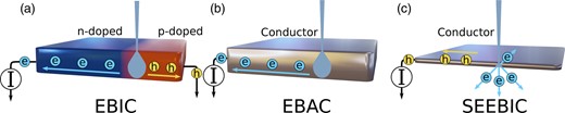
Schematics of the most common EBIC concepts. (a) An incident e-beam excites holes and carriers in the depletion region of a p–n junction, resulting in a current through the transimpedance amplifier. (b) An incident e-beam is absorbed by a conductive specimen resulting in a current through the amplifier. (c) An incident e-beam generates SE emission from a thin specimen resulting in a hole current through the amplifier.
By adopting these different naming conventions, we aim to clearly delineate the main contrast formation mechanism—whether e–h pairs are generated, electrons are absorbed from the e-beam, or current arises from SE emission. Combinations of these effects cannot, in general, be neglected; however, the naming convention captures the main contrast formation mechanisms. There is also the possibility for currents to arise elsewhere and contribute to or be attributed to an e-beam-induced process, for example, when bias voltages are applied.
It should be noted that each of these mechanisms is dependent upon beam/specimen interactions, electrical connections within the sample, and electrical connections to the sample. For example, EBAC is only possible when the e-beam—or some measurable fraction of the e-beam—can be stopped within the conductive portion of the specimen. This is typically not possible during high accelerating voltage STEM imaging where almost all the electrons transmit through the sample. Likewise, SEEBIC requires the ejection of electrons from the surface, which only occurs within several nanometers of the surface. SEEBIC can attain higher imaging resolution because of the limited interaction volume, but this is at the expense of less signal current.
SEEBIC Imaging
As mentioned in the Introduction, STEM-SEEBIC allows probing material properties including topology, work function, electrical connectivity, and SE emission (Hubbard et al., 2020). Because it is performed in a STEM, the tightly confined e-beam confers high spatial resolution. Crucially, SEEBIC differs from ADF imaging in that image contrast is generated from interactions with electrons in a sample as opposed to the nuclei. Most electrons are correlated strongly with the atomic nuclei, but delocalization of the electrons is possible as, for example, the conduction electrons in a metal or semiconductor. This can sometimes confound the interpretation of SEEBIC images compared to interpreting ADF images. While in situ electrical biasing techniques also permit electrical characterization in the microscope, SEEBIC is distinguished in its ability to probe disconnected circuits.
SEEBIC is similar to SE-STEM imaging in that an image is formed by scanning a focused e-beam over a sample and generating SEs; however, it differs in two key ways. First, while SEs are generated any time the beam interacts with the specimen, SEEBIC permits the selective examination of SEs emitted from a region electrically connected to the amplifier. This constraint is advantageous for visualizing electrical connectivity. Second, SE-STEM uses a detector that only captures a portion of the emitted SEs, sampling a small area, whereas SEEBIC typically captures a signal from all the SEs emitted, providing a detection efficiency of unity (assuming that the entire area under examination is electrically connected to the amplifier). This makes SEEBIC a more straightforward strategy for examining total SE emission and the SE yield. The requirement for a conductive path for SEEBIC does limit the types of samples that can be studied; however, as long as transport can occur, including through leakage current and other transport mechanisms, SEEBIC can be performed.
There are subtle factors that influence STEM-SEEBIC contrast. These factors also complicate SE imaging in both STEMs and SEMs, as will be discussed below, but these aspects are more prominent in SEEBIC. Most of these effects arise from the interaction of the conductive SE-generating region with the (sometimes) higher SE-generating dielectrics. Mechanisms such as electron hopping and tunneling permit the exchange of electrons over “short” distances, which are well within the regimes probed by modern aberration-corrected STEMs.
Previous Work
The most comprehensive and descriptive previous work is from 2018 (Hubbard et al., 2018) that clearly describes what is now recognized as SEEBIC and presents a clear case that distinguishes this technique from more traditional forms of EBIC. Another notable report was published in 2020 (Hubbard et al., 2020) that builds on work from the previous report and demonstrates the technique of STEM-EBIC, including SEEBIC, and shows that by using clever device design and focused ion beam (FIB) sample preparation, regions of interest in devices can be selectively extracted and analyzed with SEEBIC. A significant advance in 2019 showed that 2 Å resolution was achieved with SEEBIC (Mecklenburg et al., 2019b). In this work, lattice-resolution images were acquired of Au nanoparticles on silicon nitride membranes. A recent publication in 2021 showed that the SEEBIC technique was sensitive enough to distinguish single layers of suspended graphene, despite its very low SE yield (Dyck et al., 2021b). Utilization of the SEEBIC technique for characterizing graphene-based nanoelectronic devices was also presented in 2021, where the authors noted SEEBIC-based detection of conductance switching in graphene nanoconstrictions (Dyck et al., 2021a).
Another publication is notable for implementing resistive contrast imaging (RCI) to study a component from an actual device, in this case a multilayer ceramic capacitor (MLCC) (Hubbard et al., 2019). The authors visualized resistive grain boundaries in a sintered polycrystalline BaTiO3 dielectric layer from a capacitor, demonstrating heterogeneity in the material, which has implications for device performance such as reliability and the dielectric constant. The work shows how conductivity variations within a specimen, along with an understanding of the charge production mechanism, can facilitate mapping the resistivity of a thin specimen with high spatial resolution that not only improved the resolution previously demonstrated with RCI using EBAC (Russell & Leach, 1995) but also demonstrated how SEEBIC enables RCI in STEM, whereas EBAC is not possible due to the low absorption probability.
In another experiment, STEM-EBIC was used to study perovskite solar cell components in situ using protective electrodes for air-sensitive specimen components (Duchamp et al., 2020). This report focuses primarily on the induced current generation mechanisms. The authors have a narrower definition of EBIC, defined as charge carrier generation in an electrically contacted semiconductor device (traditional EBIC), but acknowledge and describe contributions to the signal from SEs. The relative contributions of the SE signal are separated from the top and bottom of the sample, which they were able to independently probe and show that the EBIC signal in the STEM matches surface-sensitive SE imaging in an SEM, thus verifying the contribution of SEs to the total EBIC signal.
These and other related STEM-EBIC studies (Sparrow & Valdrèg, 1977; Fathy et al., 1980; Brown & Humphreys, 1996; White et al., 2015) provide a sense for the current status of the field. The most significant developments of importance to the present work have been briefly described, providing the foundational understanding that is built upon here.
Results
Having described the current state of developments and research in the field, a number of experiments and observations using SEEBIC for the examination of graphene nanoelectronic devices will be presented. These are divided into the following sections: in the “Materials and Methods” section, sample fabrication, preparation, and acquisition details are described; in the “Imaging Supported Graphene” section, we show that a single layer of graphene is easily detected when supported on a SiNx substrate; in the “Substrate Contributions” section, the role of the substrate in generating the observed SEEBIC contrast is discussed; in the “In Situ Device Diagnostics” section, we show how the SEEBIC technique can be leveraged to reveal electrical connectivity; in the “Influence of Voltage Bias on Image Contrast” section, a series of electrical biasing experiments are presented and the SEEBIC contrast is examined; in the “Resistive Contrast Imaging” section, evidence for RCI in supported graphene is presented.
Materials and Methods
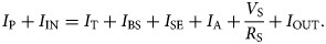
Schematic overview of the device architecture. (a) View of the full chip that interfaces with the electrical holder via the contact pads. (b) Zoomed in view of the central region which is back etched to create an electron transparent SiNx window to allow imaging in the STEM. (c) Zoomed in view of a graphene nanoribbon device between two electrodes, a portion of which is suspended across an aperture in the SiNx membrane.
STEM-compatible chips that allow electrical biasing of samples are commercially available through several companies (e.g., Hummingbird, DENSsolutions, and Protochips). Likewise, custom-fabricated substrates for the design and operation of experimental devices is increasingly common (Radisavljevic et al., 2011; Wang et al., 2012; Xu et al., 2013; Vahapoglu et al., 2021). Device integration with electron-transparent windows and examination under high resolution in STEM is also routinely performed by some research groups (Fischbein & Drndić, 2007; Puster et al., 2013; Qi et al., 2013, 2014; Rodríguez-Manzo et al., 2016; Masih Das & Drndić, 2020). This kind of architecture allows highly resolved imaging and other TEM and STEM characterization modalities to be used for examining the as-fabricated devices. By using an electrical contacting STEM holder, the device can also be operated during examination to correlate structural and electronic properties. In this work, we discuss how STEM-SEEBIC can be used to gain additional electronic information about the devices and the interpretation of various aspects of SEEBIC image contrast. It should be noted, however, that the SEEBIC technique is not limited to these devices and only requires that an electrical connection be made from a current amplifier to the sample.
Imaging was performed using a Nion UltraSTEM 200 operated at 60, 100, and 200 kV accelerating voltages (as indicated in the text). Beam currents are also listed individually. The nominal convergence angle was 30 mrad. To facilitate electrical contacting, a Protochips™ electrical contacting holder was used. A custom-built SEEBIC acquisition platform was used to record the SEEBIC signal, consisting of a break-out box to make and break electrical connections to the sample and a Femto DLPCA-200 transimpedance amplifier (TIA). All SEEBIC images were acquired with a gain of 1011 V/A and a bandwidth of 1 kHz. The TIA output was connected to an unused analog input of a Gatan DigiScan to facilitate the parallel acquisition of SEEBIC and high-angle annular dark field (HAADF) signals. Since digitization of the signal by the DigiScan system is opaque, the numerical value of the image intensity is not directly interpretable as a measured current. To obtain quantitative current measurements, the TIA output was disconnected from the DigiScan system and connected to a custom-built data acquisition platform (Sang et al., 2016, 2017; Li et al., 2018) to scan the e-beam and record the various signal outputs. Analysis of the images acquired with this custom-built system are shown with intensities of pA, whereas analysis of the images acquired with the DigiScan system are shown with intensities of arbitrary units (a.u.).
The SEEBIC signal exhibited a significant interference component, which was synced with the electrical mains manifesting as vertical stripes. This signal was removed from all images presented here in a procedure fully described in the Supplementary Information of a previous publication (Dyck et al., 2021a, 2021b). Briefly, a script was used to sum the images vertically and obtain a moving average that represents the larger-scale image features (background intensity). The background signal was removed by dividing the original signal by the background. The remaining signal represents the interference pattern to be removed. The original signal was then divided by the interference signal to obtain a corrected version of the SEEBIC image.
Analysis of the EELS data was performed using Quantifit (Tian et al., 2019). A Hydrogenic cross-section was used to model the core-loss edges, and a polynomial was fit to the pre-edge background (75–95 eV). Near-edge regions were excluded from the fit, 96–161 eV for Si, 278–293 eV for C, and 396–426 eV for N. The energy dispersion was set to 0.22 eV/channel, and data were acquired with a nominal convergence angle of 30 mrad and a collection angle of 32 mrad.
Imaging Supported Graphene
SEEBIC images are largely amenable to intuitive interpretation, especially when focused on the conductive elements; however, there are subtle aspects that should be included. Here, new interpretations of previous SEEBIC results are introduced that are more readily understood because of the 2D nature of graphene. This section will provide clarity for image interpretation by detailing the mechanisms behind image formation and contrast.
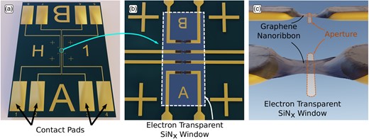
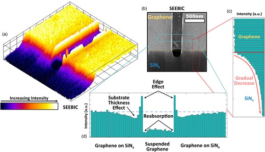
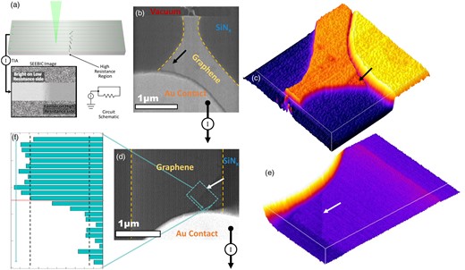
A graphene ribbon device, partially suspended and severed from contact with the bottom electrode, showing several image contrast mechanisms. (a) Grayscale SEEBIC image showing the grounded and contacted electrodes and (b) concurrently acquired HAADF-STEM image. (c) Profile across the device showing the ability of SEEBIC to distinguish graphene on SiNx, suspended, and grounded contact. (d) 3D surface plot of (a) highlighting differences in signal. (e) Histogram of SEEBIC intensities in pA from various regions. (f) Mean current for various regions. Image is 200 × 200 pixels, acquired at 60 kV with 89 pA beam current and a 15 ms pixel dwell time.
Second, the connected Au electrode is bright, as is common in ADF imaging, but the grounded electrode has the same intensity level as vacuum. The dark contrast of the grounded electrode can be explained by the fact that when the e-beam strikes this electrode, SEs are generated, but electrons are replenished by a direct connection to the common ground (not through the TIA), and therefore, no current is measured.
Third, the graphene has a lower SEEBIC signal in suspended regions compared with supported regions. This difference in contrast, shown clearly in Figures 3c, 3e, and 3f, has a less intuitive explanation as it is due to the substrate contribution of the supporting SiNx, which we will discuss in detail in the next section. Another subtle feature is a lack of sharp contrast between the graphene and the SiNx substrate, which is another substrate contribution to the SEEBIC signal.
Finally, a strong signal at the edge of the aperture is an additional feature present in the images that will also be explained in the next section but can be understood as the same edge effect observed in common SEM imaging (Seiler, 1983).
To better visualize the SEEBIC signal, a 3D surface plot is included in Figure 3d; this highlights the lack of a defined edge at the graphene/substrate interface and shows the difference in the SEEBIC signal between the Au electrode and supported graphene. To put these intensities on a quantitative footing, we analyzed the intensities as follows. The SEEBIC image was segmented into different categorical regions based on feature finding using the trainable Wekka segmentation plugin in Fiji (Schindelin et al., 2012; Arganda-Carreras et al., 2017). Histograms for each region are shown in Figure 3e. The mean values are compared in the bar chart, as shown in Figure 3f, with the standard deviation shown as error bars. The mean vacuum signal was used as a zero reference and all intensities (current values) were adjusted so that the mean vacuum reading was zero. The closest distinct signals are those of the substrate and vacuum and, as anticipated, a direct overlap exists between the SEEBIC intensity for vacuum and the separately grounded contact. The mean current values obtained for each region are listed above the corresponding bars in pA. We note that this suspended graphene is not clean graphene and thus the SEEBIC intensity is significantly increased. A previous publication measured an approximately fourfold increase in signal from contaminated regions (Dyck et al., 2021b).
Substrate Contributions
The relative SEEBIC image intensity decreases when graphene is suspended compared to locations where it is supported on the substrate. One might assume that dielectric materials would not contribute to SEEBIC contrast formation and can therefore be neglected from further consideration, but this is not the case. In this section, the contribution of the substrate to SEEBIC imaging is examined and the likely mechanisms are proposed. First, it is worth noting that substrate contributions to SE signals from nanomaterials have been discussed and debated in the context of SEM imaging. Substrate contributions are more substantial when the specimen being imaged is comprised of a single atom, atomically thin layer, or otherwise has a dimension on the order of <5 nm, which is the approximate escape depth of SEs.
In 2010, a controversial report published an anomalously high SE emission from carbon nanotubes (Luo et al., 2010). Shortly after, a comment was published by another group, suggesting that the images used to support this claim were misinterpreted and that the electrons emitted were likely coming from the substrate, with the carbon nanotubes able to replenish the substrate electrons in the vicinity, accounting for a larger SE yield from that region (Alam et al., 2011). In their conflicting study of the SE yield of multiwalled carbon nanotubes (MWCNTs), they suspended the MWCNTs and obtained a much lower SE yield. The original group published a response (Luo et al., 2011). The underlying debate concerns the role of the substrate in the SE emission process. Challenges regarding the interpretation of substrate effects are not limited to this one instance (Park et al., 2010; Park & Ahn, 2015). A common mistake is that when SEEBIC is used to probe conductivity, only ohmic conductivity is considered, whereas in reality, all forms of conduction, especially those typically considered leakage current, also play a role.
With new experimental data from STEM-SEEBIC, additional insight can be provided. Figure 3 shows a SEEBIC image of graphene suspended across an aperture in the thin SiNx membrane. In the suspended regions, substantially lower current is observed compared to the supported regions. This difference is clearly highlighted in the line profile in Figure 3c and the quantitative comparisons shown in Figures 3e and 3f.
Conduction should be examined through the lens of the graphene/SiNx/e-beam system. Silicon nitride is a dielectric with a resistivity in the range of 1010–1017 Ω-cm (Joshi et al., 2000). The wide range can be attributed to differences in stoichiometry, quality, and stress, which can drastically vary the resistivity likely through Poole–Frenkel (PF) transport (Blázquez et al., 2014) and can result in orders of magnitude differences in resistivity for relatively small changes in stoichiometry (Habermehl & Carmignani, 2002). Additionally, silicon nitride has a band gap of ~5 eV; however, this can decrease to ~2 eV with increasing Si content. Here, experiments used Si-rich SiNx; thus, it is reasonable to assume that the band gap was between 3 and 4 eV (Tan et al., 2018). The conduction of current in such an insulator, with fields below the band gap, is expected to be very small; however, this should not be interpreted as completely prohibiting the conduction of current, particularly at high electric fields (Blázquez et al., 2014) such as those generated by extreme charging of a material due to the emission of SEs. The local electric field induced by the e-beam is not known; however, given the number of SEs emitted from such a small region of material, it is reasonable to assume that it is sufficiently high (Jiang, 2016) to permit PF conduction. When a high electric field is applied, several conduction mechanisms become possible, such as PF conduction (sometimes called PF emission), hopping conduction, and tunneling over distances of a few nanometers. Studies of metal–insulator–metal (MIM)/silicon-rich SiNx show that when a 10 V bias is applied across a 20 nm thick membrane, a resistivity of approximately 103 Ω-cm is measured (Graf et al., 2019).
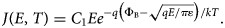

(a) Common band diagram of a MIM stack demonstrating PF emission and (b) detailed band diagram demonstrating PF emission, where qΦ is the ionization potential and β√E is the amount by which the trap barrier height is lowered by the applied electric field (E) and β is the PF field-lowering coefficient.
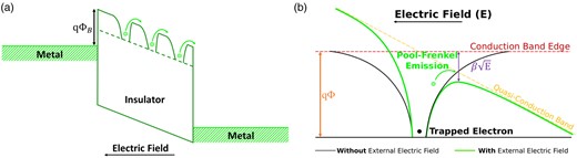
Schematic showing how an insulating substrate with a conductive layer on one side, such as graphene, can contribute to the SEEBIC signal through localized charge transport. (a) Primary beam-emitting SEs from both graphene and the substrate. This generates holes that are replenished by electrons from ground through the TIA. (b) Migration of charge resulting in a measured current through the TIA. (c) Schematic showing SE-emitting regions of the device in red, which occur primarily at sample surfaces. (d) Schematic showing SE emission as a function of both primary electrons and backscattered electrons from within the distance, λ.
Schematic showing the mechanisms behind the different intensities measured in SEEBIC images as the graphene transitions from supported to suspended. (a) When the e-beam is on the graphene on SiNx, signal comes from SEs emitted from both graphene and the SiNx; (b) at the edge of the SiNx, electrons can also be emitted from the full thickness of the SiNx, resulting in a substantially higher SE signal; (c) when the e-beam is on the suspended graphene, only the graphene and any contamination contribute to the SEEBIC signal; (d) finally, as the e-beam is on the graphene, but near the SiNx, some SEs (approximately ¼) will have a trajectory that leads them to be absorbed by the substrate, resulting in a decreased signal.
Lateral conduction in the substrate. Images acquires at 60 kV. (a) 3D surface plot showing the increase in the SEEBIC signal toward the graphene, (b) grayscale SEEBIC image showing the drop-off in contrast away from the graphene on the SiNx, (c) integrated line profile of the intensity showing SEEBIC signal over 100 s of nanometers, and (d) integrated line profile across the aperture.
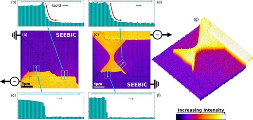
300 × 300 pixel images acquired at 60 kV and 57 pA beam current with 2 ms dwell time. (a) SEEBIC image of an electrically discontinuous graphene device with the electrical contact shown, (b) integrated line profile of graphene edge to SiNx showing gradual transition, and (c) integrated line profile of contacted graphene to grounded graphene, showing abrupt transition. (d–f) same as (a–c) with TIA and ground connections reversed. (g) 3D surface plot of (d) where the regions of substrate contributions are readily visualized.
This demonstrates that e-beam-induced transport in substrates is non-negligible in SEEBIC studies. The implications of these findings also extend beyond SEEBIC to SE-STEM imaging in general.
Diagnosing Devices In Situ via SEBIC
In a previous publication, we showed how the SEEBIC technique could be used to probe conductivity and connectivity as a diagnostic tool in the examination of graphene nanoelectronic devices (Dyck et al., 2021a). In that publication, it was clear that electrical continuity could be probed with high spatial resolution, which is useful in diagnosing simple device failure modes, such as for the electrically discontinuous graphene device shown in Figure 8.
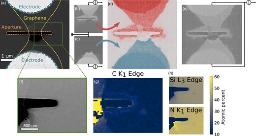
SEEBIC diagnosis of device failure. Images acquired at 60 kV and 58 pA beam current. (a) HAADF-STEM image of the device with various features labeled. (b,c) 300 × 300 pixel SEEBIC images acquired with the TIA connected to the top side of the device, while the other is grounded, (b), and vice versa, (c). Pixel dwell time was 2 ms. (d) Artificially colored composite of (b,c). (e) Both sides connected to the TIA showing that the central portion of graphene device is no longer electrically connected. (f) HAADF-STEM image of the EELS acquisition location. (g) Relative quantification of the EELS C–K core loss edge. Color corresponds to atomic percent relative to the Si and N EELS edges. The C track around the edge of the aperture is clearly visible. (h) Corresponding quantifications of the Si-L2,3 and N–K EELS core loss edges. The color bar corresponds to all three EELS images.
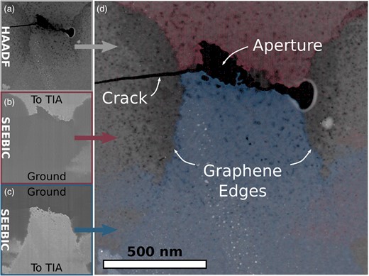
Example of how simultaneous HAADF/SEEBIC imaging can help understand device failure. (a) Grayscale HAADF-STEM image, (b) SEEBIC image of the top half of the device, (c) SEEBIC image of the bottom half of the device, and (d) false-colored composite image showing how the conductive graphene aligns with the substrate damage, providing evidence for graphene edge-associated damage at high current densities. 512 × 512 pixel images acquired at 200 kV, approximately 600 pA beam current, and 0.3 ms dwell time.
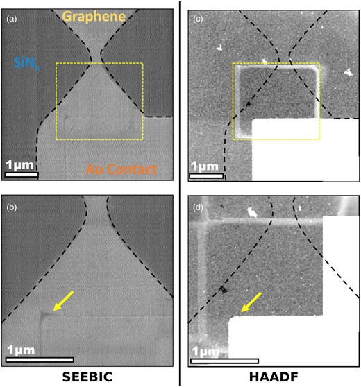
Example of SEEBIC being used to confirm that contamination is not in contact with the graphene. 300 × 300 pixel images acquired at 60 kV, 49 pA beam current, and 2 ms dwell time. (a) SEEBIC image of graphene device on SiNx and (b) higher magnification SEEBIC image. (c,d) HAADF-STEM images, where contamination on the backside of the device is clearly visible, does not appear in the SEEBIC images.
Another interesting feature in these SEEBIC images is the existence of a dark region in the graphene at the corner of the metal electrode (indicated by the arrows in Figure 11). The HAADF-STEM image gives no indication that this region is any different from the rest of the contact edge. A likely explanation is that there is a portion of graphene that is suspended as it stretches from the Au contact to the SiNx surface. In Figures 3 and 7, the signal from suspended graphene is lower than that from the supported graphene due to substrate contributions. Likewise, in Figure 3, a pronounced decrease in SEEBIC intensity is observed at the border between the TIA electrode and the graphene on SiNx. This is consistent with the idea that the graphene in this region is suspended above the contour formed between the electrode and the SiNx substrate. Moreover, this decrease is not consistently observed from one sample to the next or from one location to another, as shown in Figure 11, which is also to be expected if this phenomenon is a result of graphene suspended above the substrate. This data is not conclusive, but it is suggestive and provides enough impetus to explore this possibility further.
Influence of Voltage Bias on Image Contrast
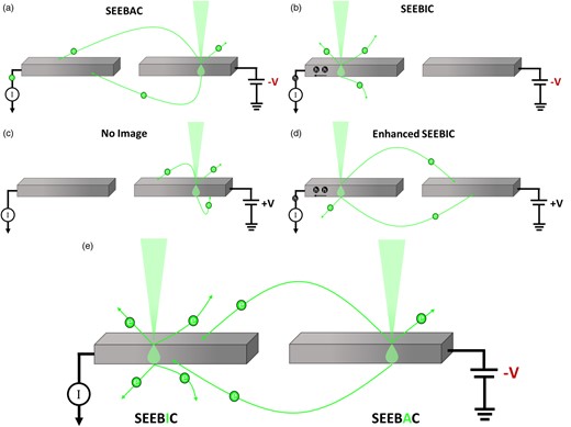
Schematic demonstrating the different forms of imaging possible with two disconnected contacts and a voltage source. (a) The e-beam is incident on a negatively biased specimen and the TIA is connected to an adjacent but electrically disconnected collector. SEs can be absorbed and an image can be formed. (b) The e-beam is incident on the sensing/TIA electrode and the opposite/non-sensing portion of the specimen is negatively biased. Normal SEEBIC imaging occurs. (c) The e-beam is incident on a positively charged non-sensing (disconnected from the TIA) portion of the specimen. Most SEs are recaptured and no image is formed. (d) Enhanced SEEBIC resulting from the positive bias, reducing recapture of emitted SEs. (e) SEEBIC and SEEBAC occurring under the same sample conditions as a result of e-beam position.
To experimentally demonstrate SEEBAC, devices were fabricated as previously and then Joule heated to clean the devices, cause SiNx substrate evaporation, and finally separate the graphene ribbon at the constriction. A computer controllable voltage source was utilized to apply a bias to one half of the device.

(a–c) False color SEEBIC images acquired with bias voltages of −10, 0, and +10 V applied to the electrode on the LHS and the TIA connected to the RHS. The displayed intensity range is the same for all three images to facilitate direct comparison. (d) Simultaneously acquired HAADF image. (e) Integrated line profiles from SEEBIC images (a–c) taken from the areas shown by dashed rectangles. Schematic with the electrical connections overlaid. Images were acquired at 200 kV, approximately 600 pA beam current 300 μs dwell time and are 512 × 512 pixels.
Figure 13d clearly illustrates both SEEBAC and enhanced SEEBIC through a comparison of line profiles taken from the locations indicated by the dotted boxes in panels (a–c). When the LHS side was biased negatively, SEEBAC occurred at the edge of the biased graphene, which is clear since the signal is lower than that of vacuum. When the polarity was switched, no difference was observed between the biased side and vacuum, but an enhanced signal from the RHS electrode was observed when compared to zero bias, suggesting that recapture is suppressed and the best possible SEEBIC imaging conditions have been achieved.
Resistive Contrast Imaging
Evidence for graphene grain boundary identified by RCI. (a) Schematic illustrating the concept of RCI, where regions with lower resistivity and higher resistivity paths to ground are brighter and darker, respectively. (b) SEEBIC image of a device where a portion of the graphene is clearly darker, (c) 3D surface plot showing the same region indicated by the black arrow. (d) Different devices showing the same behavior, (e) 3D surface plot of the same device with arrow indicating boundary, and (f) integrated line profile illustrating the drop in the intensity across the boundary. Image in (b,c) is 300 × 300 pixels and was acquired at 60 kV, 51 pA beam current, and 2 ms dwell time, (d,e) at 60 kV, 74 pA beam current, and 100 ms dwell time.
One reason STEM-based RCI has been infrequently reported is that the most common EBIC RCI mechanism is EBAC, which relies on absorption of the primary beam electrons. This is essentially a physical impossibility in the STEM due to the high accelerating voltages and ultra-thin, electron-transparent specimens used; however, RCI can also be performed using SEEBIC instead of EBAC (Hubbard et al., 2019). Both EBIC, EBAC, and SEEBIC all generate a signal, which when connected via external circuits can permit RCI. Knowledge of the type of induced current as well as the circuit configuration (e.g., grounded on both sides or biased on one) are necessary to properly interpret the images produced. One must also be cautious in interpreting the images since a change in contrast may be due to a discrete change in series resistance or a change in the entire circuit. Figure 14a illustrates this case, where the entire RHS of the specimen has a lower contrast despite the high-resistance region being confined to a specific point. From an RCI perspective, the SEEBIC analysis of graphene can be re-examined. It is well known that graphene grain boundaries represent high-resistance regions in an otherwise low-resistance material (Clark et al., 2013). The presence of a grain boundary could theoretically be detected with RCI in the STEM using SEEBIC as the charge generation mechanism, as demonstrated by the two examples of graphene devices exhibiting an abrupt change in SEEBIC contrast as shown in Figure 14.
Unfortunately, the regions of graphene were supported on the SiNx substrate, so it was not possible to use the atomic resolution imaging capability of the STEM to probe whether a grain boundary was present at the edge of the contrast transition. Given the transfer process of the graphene onto the substrate and the abrupt height change from the metal contact to the SiNx membrane, it is also possible that the observed feature is a crack induced during the transfer process. Nevertheless, the imaging is suggestive of a change in resistance and further experiments could establish this as a technique for 2D materials and other nanostructures and could prove particularly useful for emerging techniques to sculpt and probe nanoelectronic devices in situ (Rodríguez-Manzo et al., 2016).
Conclusions
In this work, we provided a brief overview of the current state of the field of STEM-based SEEBIC imaging. We have shown how STEM-SEEBIC may be leveraged for characterizing 2D graphene-based nanodevice structures and provided detailed observations and discussions regarding the contrast generating mechanisms at work. Specifically, we illustrated how the significant contribution of the dielectric substrate plays a prominent role in visualizing supported graphene, demonstrated how SEEBIC can be used to reveal electrical discontinuities with high spatial resolution, showed that negative contrast is generated by a reversal in the current flow with bias, and presented evidence for the detection of graphene grain boundaries or partial electrical discontinuities through the use of SEEBIC-based RCI. These observations and discussions will serve to establish a useful foundation for the STEM-SEEBIC technique and offer a productive pathway for future experiments.
Acknowledgments
This work was supported by the U.S. Department of Energy, Office of Science, Basic Energy Sciences, Materials Sciences and Engineering Division (O.D. A.R.L., S.J.) and was performed at the Center for Nanophase Materials Sciences (CNMS), a U.S. Department of Energy, Office of Science User Facility (O.D.). J.A.M. was supported through the UKRI Future Leaders Fellowship, Grant No. MR/S032541/1, with in-kind support from the Royal Academy of Engineering. The authors acknowledge the use of characterization facilities within the David Cockayne Centre for Electron Microscopy, Department of Materials, University of Oxford, alongside financial support provided by the Henry Royce Institute (Grant ref. EP/R010145/1).
Conflict of interest
The authors declare none.
References
Author notes
These authors contributed equally to this work.
